aFO-PLP Technology

aFO-PLP Technology
// What is aFO-PLP? //

SCIPTech’s new Additive Fan-Out Panel Level Packaging (aFO-PLP) Technology

A new Additive Fan Out (aFO-PLP) technology platform based on ultra high- speed additive processes, eliminating the need for polluting etching, developing and stripping steps used in today’s semiconductor packaging technologies.
  • Both small and large panel-based
  • Fully molded stress buffer layer
  • Ultra low manufacturing cost
  • Low capital expenditure
  • Low environmental impact
  • No long lead-time tooling
// Why aFO-PLP? //

Why Choose
aFO-PLP Technology?

aFO-PLP delivers a cost competitive and low capex panel level packaging suitable for mid to low resolution products, suitable for both low/mid and high volume production.

Higher Throughput

Large panel processing increases production capacity while improving manufacturing efficiency.

Lower Manufacturing Cost

Replacing of majority of serial interconnect steps by low cost high speed batch processes.

Digital Manufacturing

Fast new product introduction through avoidance of long lead-time customized materials and tooling.

Low Capex

Half the investment need compared to existing packaging manufacturing.

Scalable Manufacturing

Suitable for high mix/low volume as well as high volume manufacturing.

Future-Ready Technology

Developed with environmental concerns in mind.
// Ready to Innovate? //

Accelerate Your Semiconductor Innovation with aFO-PLP Technology

Discover how SCIPTech’s aFO-PLP packaging technology can help reduce manufacturing cost and support next generation of semiconductor packaging manufacturing in high labor cost regions.
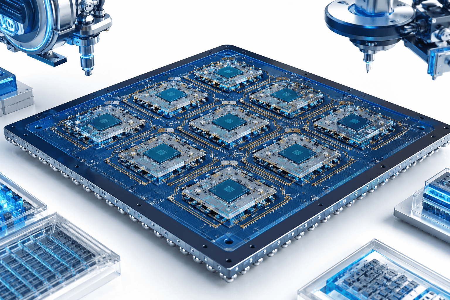
Advanced aFO-PLP Semiconductor Packaging Technology